As promised last time we're here completing the multi-vibrator astable cycle with a test on breadboard.
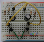
Here beside a from-top photo of a base pull-up set (i.e. resistors go from positive supply to bases. Pull-downs start from ground).
Very quickly: some screenshots from oscilloscope will reveal what indeed we've discovered with an on-chart look.
The present post doesn't cover deep technical details but tends to give a consistent view about what happens with a real astable circuit.
Jelly-beans parts are used so that it's easy and cheap for everybody to replicate it in a quick.
In this case the bjts are two npn BC548C, very common low power amplifying transistors here used in switch mode; then two 1k resistors (1/4 W) going from the positive rail to the collectors; other two 10k resistors (1/4 W) for the bases and finally the 100μF 25V electrolytic caps which go from the bases to the opposite collectors through the yellow wires.
Tests were performed with two values of power supply: 5V and 13.5V.
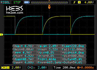
Here's what obtained with 5V:
They are the "same" screenshots, with channel1 (yellow trace) reported values on left and channel2 values on right: the signals are probed at the outputs, i.e. collectors.
By confronting them you can easily look at their slight different response: channel1 (left branch in the circuit on photo) has generally a minor voltage drop and a little bit better duty cycle; as previously explained this asymmetry is the key that makes the circuit work.
Essentially the frequency is the same: 683mHz.
Notice the raising curves: when one bjt saturates and pulls its collector almost to ground then the other goes in interdiction and lets its collector voltage get up, the presence of cap clearly limits the raising time so that we can appreciate the typical exponential charging curve.
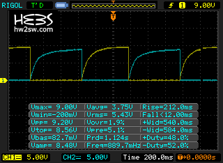
Quite the same with 13.5V power supply:

 Here the differences between branches are evident: Vmax is 10V for Ch1 and 9V for Ch2; duty cycles and frequency are clearly different.
The voltage drop for right branch (Ch2) is bigger than for left one and in general the minimum drop from positive rail to outputs is 3.5V: quite remarkable power dissipation for a circuit like this.
What is important to notice here is the difference in frequency between these two sets: before we had 683mHz and now at least 822 for Ch1 up to 890mHz for Ch2.

