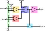

The block diagram, here reproposed, shows the pin numbers and their connections.
Beside, the picture with the physical placement of pins with relative numbers.
Standard rule wants the numbering starts from the left-top (where you find a dot or half a circle) and going on roundly.
This will help us to quickly associate the roles and behaviors they have with the real positions onto the IC.
Let's begin from the power pins: 8 and 1, respectively positive voltage and ground.
The three resistors are directly biased, resulting in a stiff double voltage divider whose points go each separately to input of comparators.
Once chosen the Vcc supply, their values are fixed. What we must expect now is that the other inputs will vary in some way.
In facts you see how the other two lines, numbered 6 and 2, goes outside the diagram block, for which they become accessible from outside.
We have our two leverages!
By looking at the comparators they give digital values in output, nothing special maybe.
The matter is they go into the FF, affecting its status by their values. In other words, they concurr to form the status of the FF, but they do one against the other.
This result is inherent to the FF nature.
So what happens?
The Trigger line goes to the inverting input: its value is compared to the one present onto the non inverting input, which is obviously 2/3 Vcc.
If it's minor then the comparator sees a positive difference between inputs and gives High value in output, if major then output is Low.
Specular situation for the above comparator: this time the fixed voltage divided value of 1/3 Vcc goes into the inverting, and the external line, pin 6 called Threshold, goes to non inverting.
The local behavior doesn't change: positive difference gives High output, while negative one gives Low.
[And if the input values are perfectly equal or difference is zero?]
Pin 4, the global Reset, has already been explained.
Pin 3 is the Output, and simply can assume value of High or Low, which are (quite) equal to Vcc and ground respectively.
Pin 7 is the discharge one; we'll see why.
Pin 5 is the Control: by setting its voltage value we change the fixed 1/3 Vcc value imposed by the voltage divider, and it can go from Vcc (even more with an external source, but there's no need of this) to... to what?
Finally, note that pin 3 and pin 7 (output and discharge) are in phase; it means that they're High or Low at the same time!
This is important for future uses.
Next time, with the S-R FF explained, we'll be able to understand the magic.
Thank you!