Maybe the most famous precision electronic timer of all times, NE555 was invented by Hans Camenzind (Switzerland) in 1970.
After more than 40 years it's still alive and healthy: born in the BJT's era now it is available in CMOS technology, even at low voltage (for more specific requirements) and in more than a package.
The interest about it never decreases, because of its simplicity and versatility.
And you'll find plenty of examples on the web with this IC involved.
By integrating both analogical and digital circuitry (very basic aspects) it is a bridge for the beginners to pass from discrete components to integrated ones with a good continuity level.

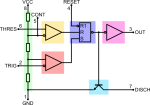
The block scheme is so clear to be quite completely auto-explicative.
We can recognize, from left to right:
- the voltage biasing network of the three 5KΩ resistors, which the name comes form;
- two comparators;
- an S-R Flip-Flop (Set-Reset);
- the output inverter;
- and the discharging transistor (on the bottom).
While the BJTs and the resistors are common to beginners, the others require at least a brief explanation; so let's start.
Comparators are integrated circuits having two voltage inputs, one inverting signed with - and the other non inverting signed with + (in figure the inverting one is indicated with a dot), and an output which gives the maximum or the minimum available voltage if value of + is major than the value of -, or viceversa respectively.
They essentially furnish a digital signal (High or Low).
Their outputs are the inputs for the S-R Flip-Flop.
A Flip-Flop is a digital device capable to keep stable a value at its output until a new value (already stably present on input) is passed through.
A so called "Table of Truth" is used to show its behavior; without getting into the details (more to come after) it gives a stable value of voltage as output, which can be again High or Low, purely digital; and that's enough for now.
By keeping this in mind we have that the inverter block of final output takes that value and change it into its opposite:
- High -> Low;
- Low -> High.
Note that the Flip-Flop has a third input line, the global Reset, which is inverted so that is activated with a Low signal.
What you have to know about it is that being global it overrides every other inputs, forcing the FF output to Low.
It must be not confused with the reset input line of the FF.
Moreover the Flip-Flop output signal drives the bottom BJT, using it as a switch, so that if the signal is High then the BJT is electrically closed and the current can flows to ground; otherwise, for Low signal, BJT is electrically open and stops the current.
(The global Reset fixes the 555 output to Low, and electrically opens the BJT - no current flowing).
By looking at the complete schematics you'll find these blocks exploded into their constitutive components as well as two other components, the current mirrors, used to power and polarize the comparators; current mirrors won't be examinated because are not fundamental to understand how the NE555 works.