In the last two articles we have worked on the breadboard.
We have seen that the circuit worked well so we need to construct it in PCB and then calibrate it.
We will start with the KiCad schematic file and then we will see the PCB layout.
Then we will construct a weight board with the load cell installed on it.
Once done with this step then we should be able to calibrate the device.
The calibration will be discussed in a next article.
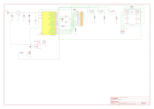
The first thing in order to construct the PCB is to design the schematic using kicad.
A series of KiCad tutorials have already been discussed here.

Above we can see the whole schematic of our liquid filler.
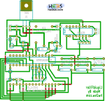
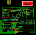
Now using the PCB tool of KiCad we have created our PCB board.

All KiCad files (schematic,netlist,pcb etc...) can be downloaded from here : Liquid-Filler-KiCad
If you only want the PCB schematic you can download it from here : Liquid Filler PCB Schematic
Now we are ready to construct our PCB board.
We have already presented the toner transfer technique that can be possibly used in order to construct your PCB board at home.
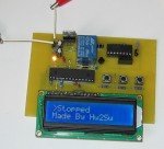
At this point you should be able to have the liquid filler board on your hands !

Now you should drill all vias at 0,5 mm and all pads at 0,8 mm drill bits.
A demonstration video can be found below.

